

 1st June 2013, 09:22
| #16 |
| BHPian | |

|

| |
|
1st June 2013, 15:07
| #17 |
| BHPian Join Date: Jun 2008 Location: Gurgaon
Posts: 97
Thanked: 157 Times
| |
|
|


|
1st June 2013, 15:24
| #18 |
| BHPian | |
|
|

|
1st June 2013, 15:35
| #19 |
| BHPian Join Date: Jun 2008 Location: Gurgaon
Posts: 97
Thanked: 157 Times
| |
|
|
|
1st June 2013, 15:38
| #20 |
| BHPian | |
|
|
|
9th June 2013, 19:05
| #21 |
| BHPian Join Date: Jun 2008 Location: Gurgaon
Posts: 97
Thanked: 157 Times
| |
|
|

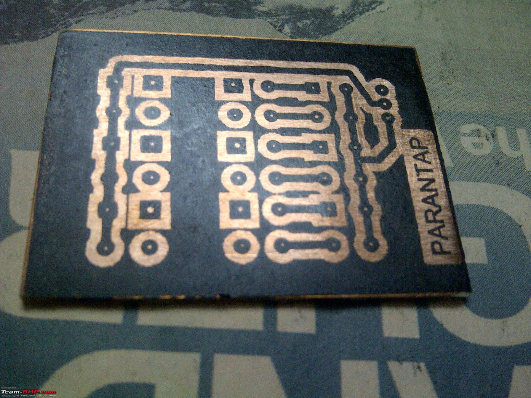
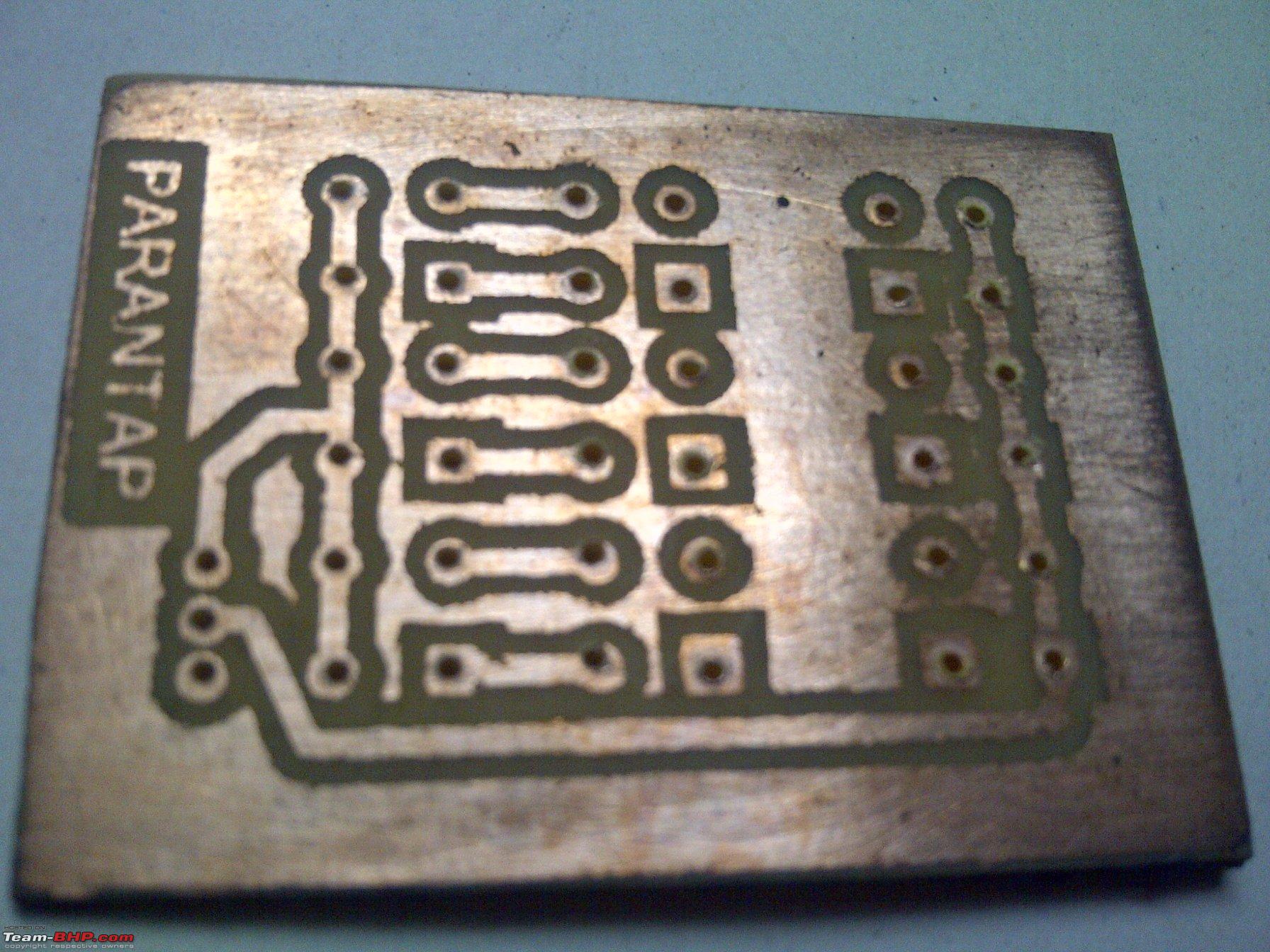
 A pre-requisite of drilling the holes accurately is that the transfer should be fairly precise so that the holes have well-defined centers. The centers are obviously etched leaving you with a dimple surrounded by copper. The dimple acts as a guide for the drill bit. Since the holes I got were warped , the drill bit wandered all over the place and actually stripped some copper for some of the holes. On the brighter side , the component placement/sizes were spot on.
 |
16th June 2013, 21:58
| #22 |
| BHPian Join Date: Jun 2008 Location: Gurgaon
Posts: 97
Thanked: 157 Times
| |
|
|  (1)
Thanks (1)
Thanks
|
|
5th November 2016, 11:50
| #23 |
| BHPian Join Date: Dec 2015 Location: Delhi
Posts: 95
Thanked: 77 Times
| |
|
|
|
5th November 2016, 12:24
| #24 |
| Senior - BHPian | |
|
|
|
8th January 2017, 02:36
| #25 |
| BHPian Join Date: Mar 2009 Location: Ghaziabad
Posts: 870
Thanked: 211 Times
| |
|
| (1)
Thanks
|
|
19th August 2020, 15:31
| #26 |
| BHPian | |
|
|
| |
|
26th August 2020, 21:13
| #27 |
| BHPian Join Date: Jun 2008 Location: Gurgaon
Posts: 97
Thanked: 157 Times
| |
|
| (2)
Thanks
|

|
26th August 2020, 22:08
| #28 |
| BHPian | |
|
|
 |